google-site-verification: google0228a1feb97d321e.html
google-site-verification: google0228a1feb97d321e.html
google-site-verification: google0228a1feb97d321e.html
google-site-verification: google0228a1feb97d321e.html
google-site-verification: google0228a1feb97d321e.html
google-site-verification: google0228a1feb97d321e.html
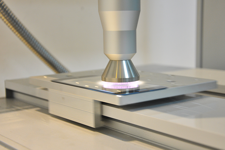
YMAPS provides innovative and efficient solutions that are determined by extensive industry experience. Plasma cleaning is a completely dry cleaning technology, without chemical pollution, secondary aromatic staining, and can be fully activated glass surface, so that the subsequent process of COB, COF, TCP, COG and other processes more smoothly completed.
Application of electrical parts:
Plasma surface activation
Surface activation prior to printing, potting and bonding Surface activation prior to preparation of conformal coatings Surface activation prior to bonding
Clean the circuit board
Water cleaning
Esd surface cleaning
Potentially free cleaning
Plasma treatment is the best solution to meet the high requirements of the industry. The cleaning process does not involve any electrical conduction, making it an ideal finish for components containing circuits. This ensures that the circuit is not subject to discharge during surface activation and surface cleaning treatments.