google-site-verification: google0228a1feb97d321e.html
google-site-verification: google0228a1feb97d321e.html
google-site-verification: google0228a1feb97d321e.html
google-site-verification: google0228a1feb97d321e.html
google-site-verification: google0228a1feb97d321e.html
google-site-verification: google0228a1feb97d321e.html
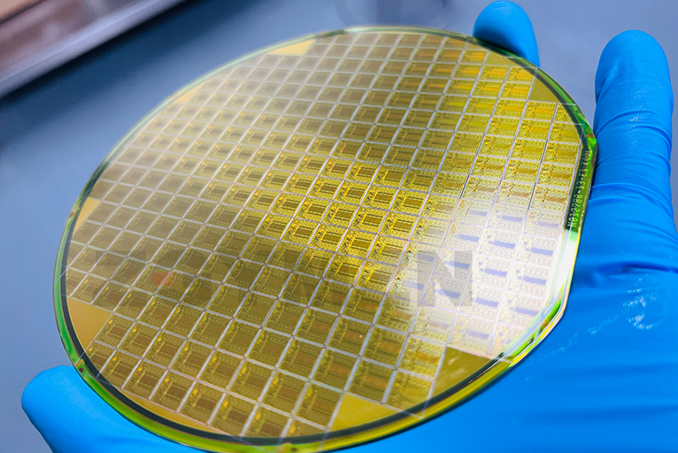
Shanghai Yangmi Technology provides unique ultrasonic spraying technology for semiconductor photoresist coating. Compared with traditional coating processes such as spin coating and dip coating, it has the advantages of high uniformity, good encapsulation of microstructure and controllable coating area. It has been fully proved that the photoresist coating on 3D microstructure surface by ultrasonic spraying technology is significantly higher than that by traditional spin coating technology in terms of microstructure encapsulation and uniformity. available Coating planar and 3D structural substrates including silicon wafers, glass, ceramics, metals, etc. Typical photoresist coating applications include wafer MEMs, lenses, microfluidic chips, filters, etc.
