google-site-verification: google0228a1feb97d321e.html
google-site-verification: google0228a1feb97d321e.html
google-site-verification: google0228a1feb97d321e.html
google-site-verification: google0228a1feb97d321e.html
google-site-verification: google0228a1feb97d321e.html
google-site-verification: google0228a1feb97d321e.html
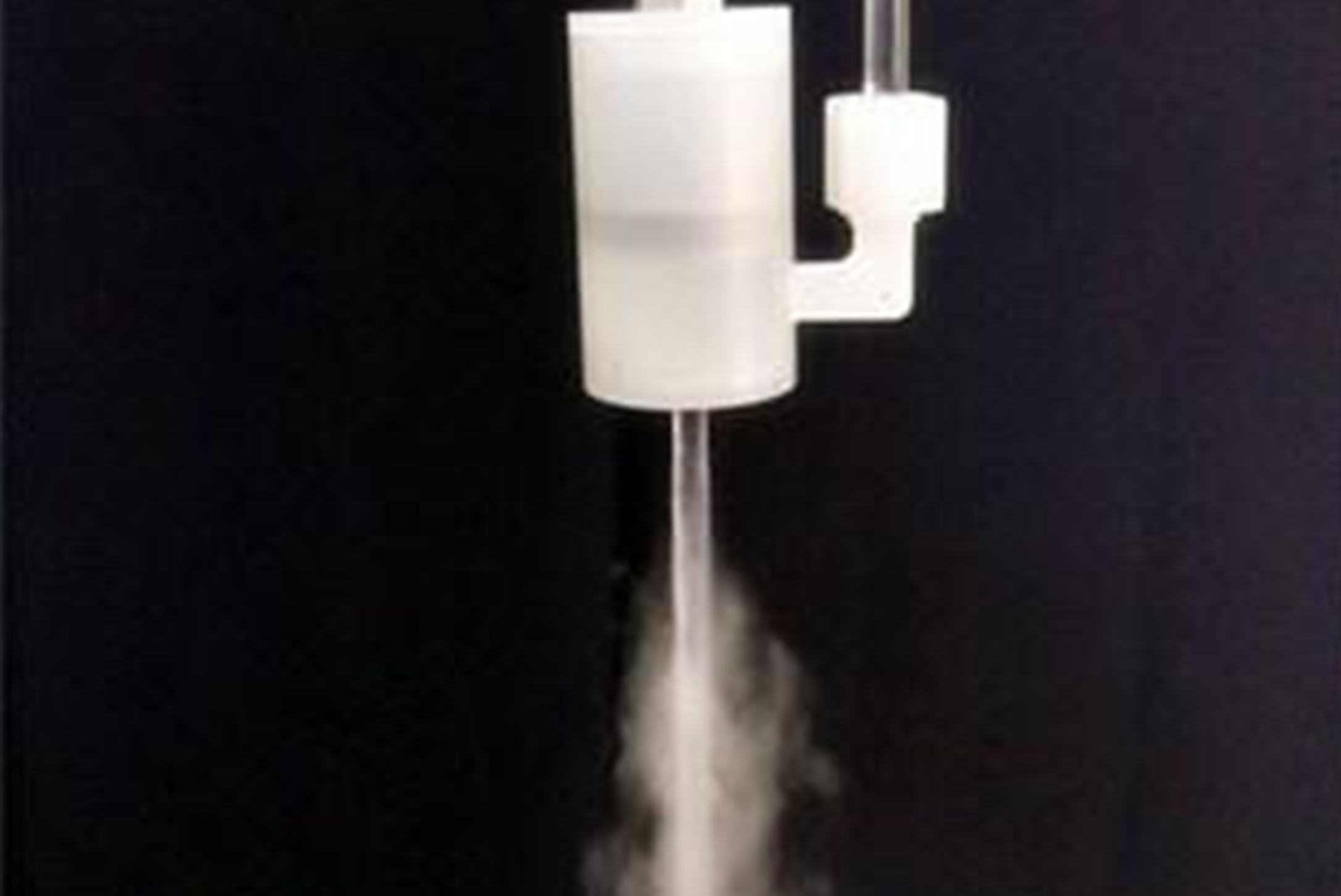
Mega wave cleaning not only preserves the advantages of ultrasonic cleaning, but also overcomes its shortcomings. During cleaning, high-energy sound waves with a wavelength of 1μm and a frequency of 0.8 MHZ are emitted by the transducer. The solution molecules are accelerated by this sound wave, and the maximum instantaneous velocity can reach 30cm/s. Therefore, the bubbles can not be formed as ultrasonic cleaning, but can only continuously impact the wafer surface with high speed fluid wave, so that the tiny particles of contaminants attached to the silicon wafer surface are forced to remove and enter the cleaning liquid.
It can remove the particles less than 0.2μm on the surface of the chip, which can not play the role of ultrasonic wave. This method can play the role of both mechanical wiping and chemical cleaning methods. The cleaning method of megabonic wave has become an effective method for polishing sheet cleaning.
Frequency above 400 KHZ ultrasonic wave travels in a liquid, can make the forming velocity gradient near the surface of the parts to be cleaned very big and very thin acoustic boundary layer, the impurity particles by the oscillation of the liquid MHZ frequency function falls off from the device surface, can clean off the components on the surface of micron, submicron level of impurity particles, realize super precision cleaning process. In addition, the high-frequency ultrasonic cleaning process will not cause damage to the surface of the cleaned parts due to the very low cavitation effect, which can effectively solve the phenomenon of corrosion or damage and destruction caused by the cleaning of precision components. So can emit megahertz level megatasal device is widely used in the field of semiconductor manufacturing, and in addition to cleaning, can also play an important role in CMP chemical mechanical polishing, development, in addition to glue, metal stripping, etching and other key processes.
Typical application areas of megabonic cleaning technology
CMP chemical mechanical polishing
Wash before bonding
Mask cleaning
developing
stripping
Lift-off metal stripping
Wet etching
The lens cleaning
Display and other microelectronics industry precision cleaning
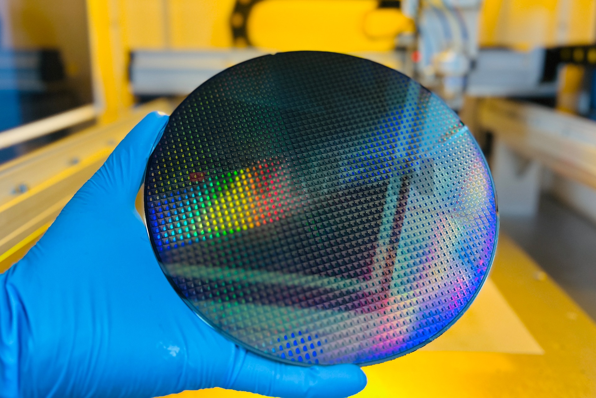
Wafer cleaning