google-site-verification: google0228a1feb97d321e.html
google-site-verification: google0228a1feb97d321e.html
google-site-verification: google0228a1feb97d321e.html
google-site-verification: google0228a1feb97d321e.html
google-site-verification: google0228a1feb97d321e.html
google-site-verification: google0228a1feb97d321e.html
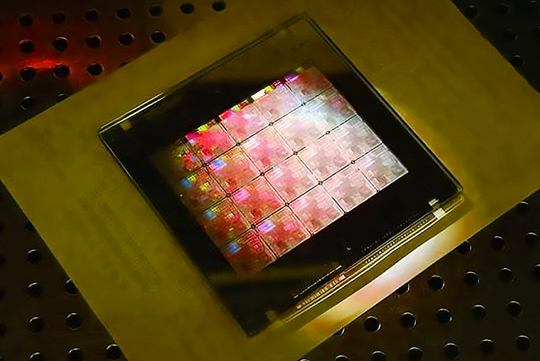
As a representative of ultra-precision cleaning nanoscale cleaning technology, mega acoustic wave cleaning technology plays a vital role in the field of semiconductor cleaning, has become a cutting-edge precision cleaning field emerging a young dark horse! It can not only clean silicon wafers (Si wafers), GaAs, liquid crystal glass and other glass masks, but also complete the ultra-precision cleaning of brittle materials such as hard disks and their read/write heads, semiconductor components, optical masks, and thin film magnetic heads. At the same time, it can handle the precision cleaning of TSV etching cleaning, UBM/RDL cleaning, bonding cleaning and other advanced packaging fields. With the further development of research, megapsonics cleaning technology is not only more and more applied in the production process of semiconductor and electronic devices, but also in the precision cleaning of optical devices and medical instruments.
The principle of mega acoustic wave cleaning
The mechanism of megabound cleaning is to clean silicon wafers by high energy frequency vibration effect combined with chemical reaction of cleaning agent. When cleaning, the transducer sends out a wavelength of megahertz high energy sound wave, and the solution molecules accelerate under the push of the sound wave, and the maximum instantaneous speed can reach 30cm/s. The megabound cleaning not only preserves the advantages of ultrasonic cleaning, but also overcomes its shortcomings. Mega acoustic wave cleaning can remove particles less than 0.1 llxm on the surface of the substrate, which can not play the role of ultrasonic wave. This method can play the role of mechanical scraping (torsion) and chemical cleaning methods at the same time. In addition, the mega wave cleaning frequency is higher, it is different from the ultrasonic cleaning of standing wave, will not damage the cleaning object. In addition, megabound has more advantages than ultrasonic wave in viscous layer thickness, power density, resonance effect and diffraction effect.
The DEVELOPMENT OF MEGA SONIC cleaning technology provides a level of wafer and mask cleaning in areas such as MEMS and semiconductors that can help users obtain the cleanest wafers and masks.
Shanghai Yangmi provides megabu high frequency cleaning machine system, advanced lossless megabu cleaning. Can be applied to easily damaged patterned or unpatterned substrates, including a mask with a protective film. In order to achieve a cavitation cleaning effect without damaging the substrate, the density of megabonic energy must be kept slightly below the damage threshold at any location on the sample. Our technology ensures that the acoustic energy is evenly distributed throughout the substrate surface, supporting cleaning by maximizing the distribution of energy while remaining within the sample damage threshold.
The characteristics of mega acoustic wave cleaning technology
(1) It can greatly reduce the thickness of the boundary layer, so that it has the ability to remove deep submicron particles, which can meet the requirements of the current process and 0.1μm (line width) technology for cleaning process.
(2) can greatly improve the cleaning efficiency.
(3) Mega acoustic wave cleaning can use large dilution of the chemical solution, so as to greatly reduce the dosage and consumption of chemicals, reduce the cost of cleaning process, effectively reduce the pollution of chemical solution, protect the environment.
