google-site-verification: google0228a1feb97d321e.html
google-site-verification: google0228a1feb97d321e.html
google-site-verification: google0228a1feb97d321e.html
google-site-verification: google0228a1feb97d321e.html
google-site-verification: google0228a1feb97d321e.html
google-site-verification: google0228a1feb97d321e.html
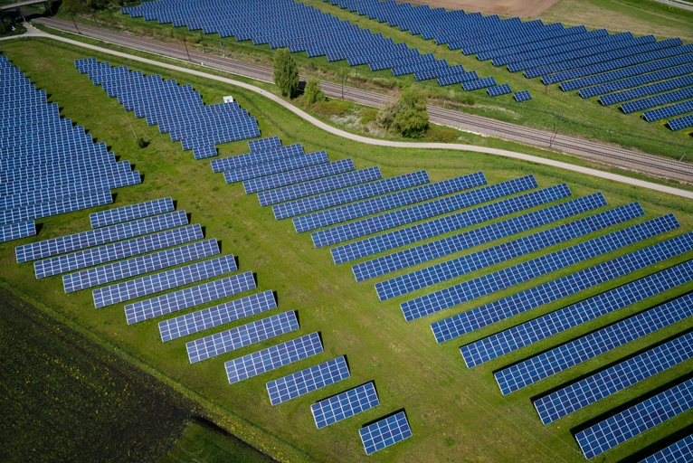
Wafer bonding technology has a wide range of applications in solar cells, various fields and rich materials. It plays an important role in the manufacturing of solar cells, improving the conversion efficiency of cells and reducing the cost. Solar cell is a kind of renewable energy that converts sunlight into electricity, which can be used in aviation, agriculture, communication, military, civil and other fields. The application of wafer bonding technology in solar cells can improve the conversion efficiency and reduce the cost of solar cells.
Wafer bonding technology can also be used to make flexible, sensing, generating power flexible solar cells. It enables the combination of multiple materials to integrate other functional materials into the solar cell, creating a variety of different functional solar cells.
Scope of application
● Si thin film solar cells
● GaAs solar cells
● Pasted solar cells
● Monocrystalline and polysilicon solar cells
● Micron and transparent solar cells
● High directional and functional solar cells
Applicable material
● Germanium
● Silicon carbide
● Zinc oxide
● Copper indium gallium selenium
