google-site-verification: google0228a1feb97d321e.html
google-site-verification: google0228a1feb97d321e.html
google-site-verification: google0228a1feb97d321e.html
google-site-verification: google0228a1feb97d321e.html
google-site-verification: google0228a1feb97d321e.html
google-site-verification: google0228a1feb97d321e.html
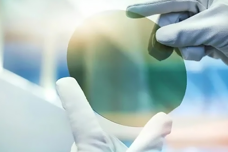
Semiconductor materials are widely used in a variety of devices, such as field-effect body tubes (MosFets, Fets), integrated circuits (IC, MMIC, ASIC), focal plane arrays, and infrared detectors. Regardless of the application or material, each semiconductor garden goes through several common stages in the manufacturing process. This includes cutting the product circles from the product body, preparing the surface before manufacturing, and thinning the device after manufacturing by using grinding and polishing techniques.
YMJH offers a complete system solution, including consumables for precise thinning of these IIVs, IR and similar materials.
Scope Application
● MEMS
● Semiconductor devices
● Semiconductor bottom
● Encapsulation
Applicable material
● Silicon-based materials (Si, a-Si, poly Si)
● III-V material (GaAs, InP, GaSb, etc.)
● Third generation semiconductor materials (SiC, GaN, etc.)
● Infrared materials (CZT, MCT, etc.)
● Photoelectric materials (LiNbO3, LiTaO3, SiO2, etc.)
● Metal materials (Au, Cu, Al, Mo, TC4, etc.)
